近年来,随着数字技术和人工智能技术飞速发展,芯片的应用领域不断拓展,在全球经济及社会发展中的重要性与日俱增。全球芯片市场需求持续增长,芯片产业从设计、制造到封装测试的产业链格局正在迅速变迁,产业链结构也在不断优化。本文将对全球与中国芯片产业链进行概要分析,供广大读者参考。
一、深度分析解读芯片产业链
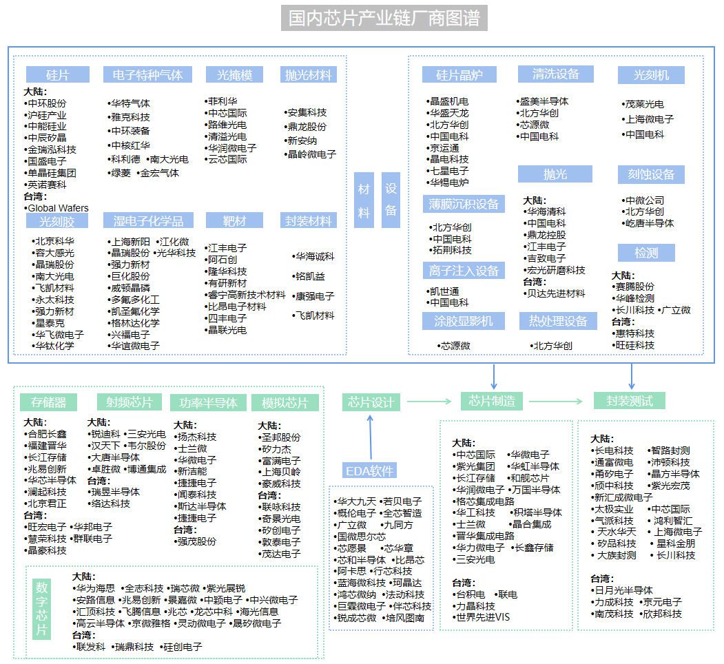
完整的芯片产业链主要包括芯片的设计、制造和封装测试主要环节,此外还衍生出包括芯片制造设备、关键材料等在内的相关支撑产业。按照上下游产业划分,芯片产业链可简单的划分为:上游包括EDA软件、芯片制造所需的材料及设备;中游为芯片设计与制造过程,包括芯片设计、芯片制造、封装测试;下游广泛应用于通讯设备、人工智能、汽车电子、消费电子、物联网、工业、医疗、军工等领域。如图1所示:
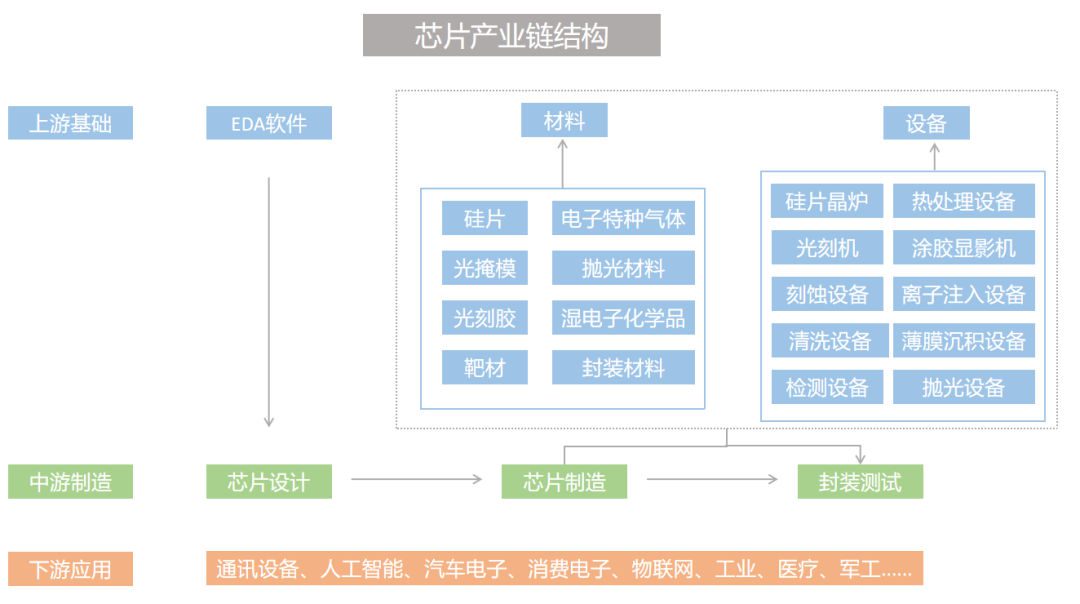
析其中,EDA软件是芯片设计的核心工具,是芯片设计和制造流程的支撑,是芯片设计方法学的载体,也是连接设计和制造两个环节的纽带和桥梁,位于芯片产业链的上游。关联视频
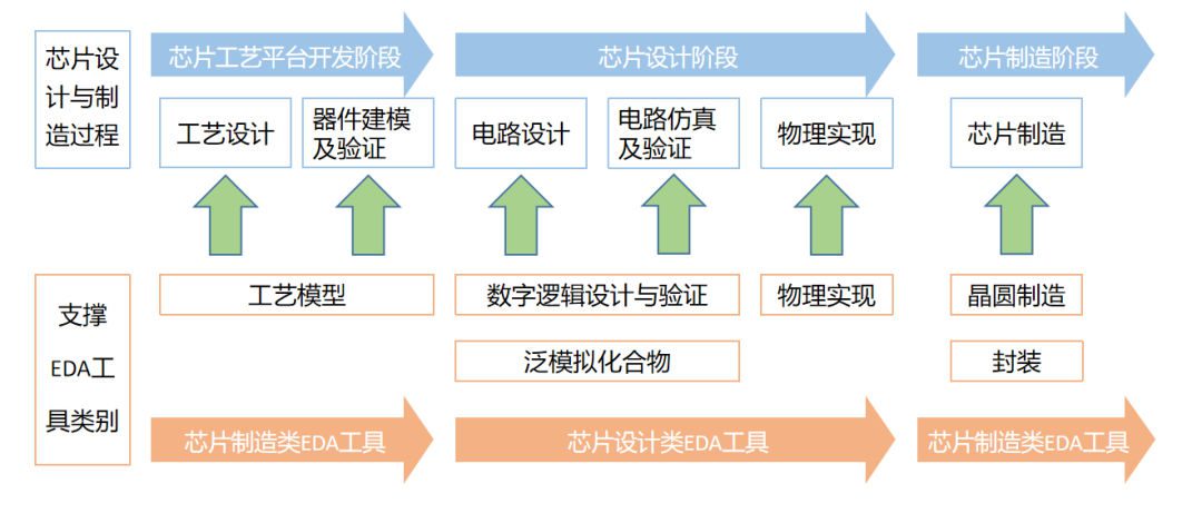
一个完整的芯片设计和制造流程主要包括工艺平台开发、芯片设计和芯片制造三个阶段。工艺平台开发阶段主要由晶圆厂主导完成,在其完成半导体器件和制造工艺的设计后,建立半导体器件的模型并通过PDK(Process Design Kit,工艺设计套件)或建立IP和标准单元库等方式提供给芯片设计企业。芯片设计阶段主要由芯片设计企业主导完成,其基于晶圆厂提供的PDK或IP和标准单元库进行电路设计、仿真验证和物理实现。芯片制造阶段主要由晶圆厂根据物理实现后设计文件完成制造。
上述三个设计与制造的主要阶段均需要对应的EDA工具作为支撑,包括用于工艺平台开发和芯片制造两个阶段的制造类EDA工具,以及支撑芯片设计阶段的设计类EDA工具。
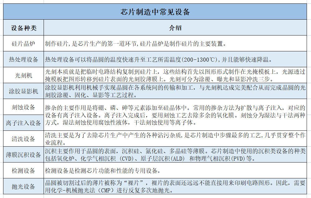
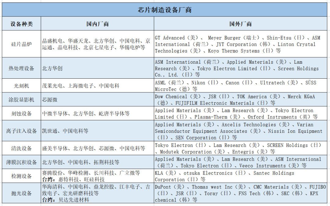
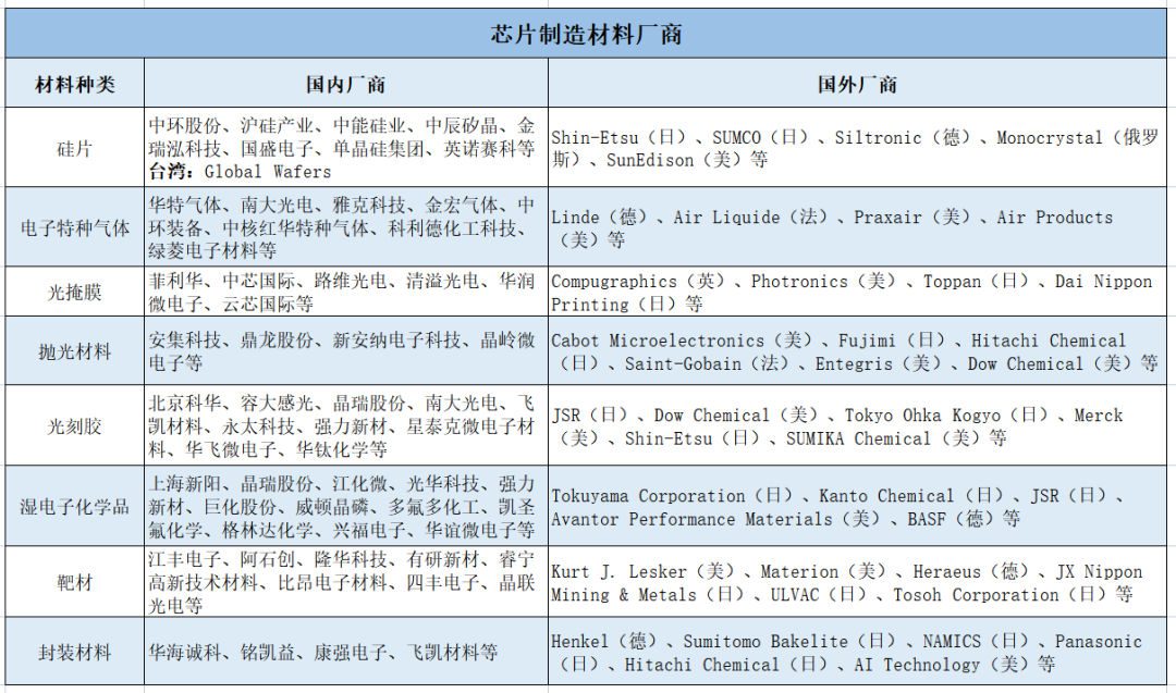
芯片制造设备和材料,是位于芯片产业链上游的另外两大重要支撑环节。在《芯片是怎样“炼”成的》一文中,我们将芯片的制造过程简单分为晶圆加工、氧化、光刻、刻蚀、薄膜沉积、互连、测试和封装八个步骤。其中所需要的设备包含了硅片晶炉、热处理设备、光刻机、涂胶显影机、刻蚀设备、离子注入设备、清洗设备、薄膜沉积设备、检测设备、抛光设备等。此外,芯片制造过程中,主要用到的材料包含硅片、电子特种气体、光掩膜版、光刻胶、抛光材料、高纯度湿电子化学品、靶材、封装材料[1]等。各设备和材料种类的介绍如下表1、表2所示。
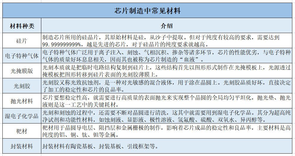
注:《对芯片分类的探讨》一文中,我们根据半导体材料类型的分类维度,归纳了三代半导体材料。其中硅和锗是第一代材料;砷化镓和磷化铟为第二代材料;碳化硅和氮化镓为第三代材料。硅是目前应用最广泛的芯片材料,大多数常见的芯片都是由硅材料制作而成。此处我们主要总结芯片制造中的常见材料,所以只归纳硅片。
芯片设计位于芯片产业链中游,芯片能实现怎样的功能主要看最初芯片的整体设计。其将系统、逻辑与性能的设计转化为具体的物理版图,包括芯片的规格制定、RTL(寄存器传输级)code实现、编码检查与分析、功能验证、逻辑综合、布局布线、静态时序分析、物理验证、功耗分析、时序仿真等关键步骤。关于芯片的设计过程,详见《数字芯片是怎样设计出来的?》一文。
封装测试是芯片产业链中游的第三个专业化环节。芯片封装的主要作用是给微小精密、易受损的芯片裸片提供一个坚固耐用的保护壳,同时把裸片上密集微小的电信号触点与封装外较大的电信号引脚或焊点相连,以便芯片可以方便地焊接在电子元件中。芯片测试通常包括两个步骤:功能测试和性能测试。功能测试是检查芯片的功能是否正常的过程,通常包括检查芯片的输入、输出,以及它们之间的逻辑连接是否正确。性能测试是确保芯片在运行时具有良好性能,包括对芯片的功耗、运行速度以及其他可能影响芯片性能的因素进行测试。
依据生产设计和制造能力的不同,芯片行业划分出三种运营模式,分别是:IDM、Fabless和Foundry。芯片行业是高技术壁垒的行业,由于芯片设计与制造包含的流程众多,芯片企业负责的环节不同,也就产生了不同的运营模式。
早期的芯片企业以IDM模式为主,IDM模式也称为垂直一体化模式,即企业同时拥有设计和制造能力[2],是一种集芯片设计、制造、封装、测试和销售等多产业链环节于一体的产业运作模式。这种产业模式可以很好地协同设计、制造等环节以实现技术闭环,有助于快速发掘技术潜力,但其运作费用较高,通常回报偏低。
随着经济的发展,一部分IDM企业开始让出部分生产环节,交给独立企业来制造,自己转型成只做设计的企业,以获得更高的利润。这种新模式称为垂直分工模式,将设计、制造和封装测试分离成芯片产业链中独立的一环。
垂直分工模式包含Fabless和Foundry模式。Fabless是指只从事芯片设计与销售,而不涉及制造、封装和测试等环节的一种产业运作模式。这种产业模式运作费用较低,投资规模较小,转型灵活,但无法做到IDM的技术协同设计,很难完成严苛的指标。Foundry即常说的“芯片代工厂”,负责生产、制造芯片的厂家,它是只负责芯片制造、封装或测试的其中一个环节,而不负责芯片设计环节的一种产业运作模式。这种产业模式不用承担市场或产品设计缺陷等决策风险。但投资规模较大,维持产线稳定运行的费用较高。
二、多维解读构建芯片产业生态
芯片行业衍生出的垂直分工模式,将芯片的设计与制造独立开来。但如今随着全球经济的变动,地缘政治因素的影响,Fabless厂商与Foundry厂商之间的关系已经不仅仅是单纯的商业委托,全球供应链的碎片化迫使我们要将芯片设计和制造能力有机结合起来,不断提升自主产业链上下游厂商的竞争力,使得芯片产业链在充满不确定性的环境下,依然能坚韧发展。那么,全球芯片产业链现状如何?各环节有哪些典型厂商做支撑?以下将重点对芯片产业链上、中游进行分析。
1.芯片产业链上游分析
EDA领域
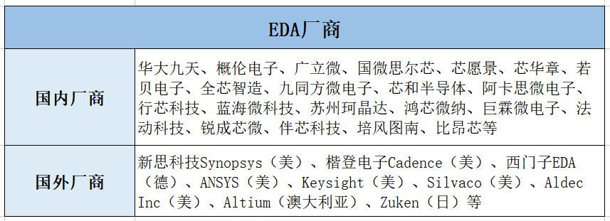
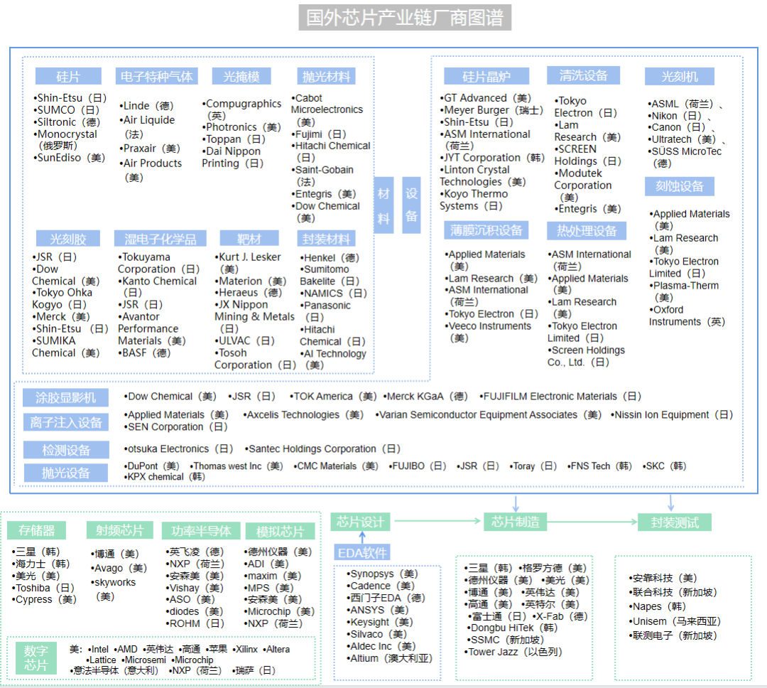
众所周知,全球EDA市场寡头垄断,集中度较高。新思科技(Synopsys)、楷登电子(Cadence)、西门子EDA(前身为Mentor Graphics,2016年被西门子收购后,2021年正式更名为西门子EDA)和ANSYS被称为EDA软件的“四大金刚”。公开资料显示,其在全球EDA市场的占比接近80%。“四大金刚”的垄断之势,或是源于其能提供完整的EDA工具,覆盖从前端设计、后端设计、仿真/验证直到流片的整套产品,形成设计的闭环;亦或是源于其在擅长的领域苦心经营,在芯片设计与制造流程的不同环节形成独特优势,发挥着关键作用。此外,国外还有Keysight、Silvaco、Aldec、Altium、Zuken等EDA厂商,在各自擅长的领域不断深耕。
虽然国产EDA厂商起步较晚,但国内芯片产业链的不断深入,使得大众对于上游EDA的关注度直线上升。随着国内芯片上下游领域的多样化发展,特别是近年来5G、人工智能、自动驾驶等新兴技术的产业化加速,以及传统制造产业转型升级,芯片需求量随之激增,中国半导体市场蓬勃发展,国内EDA的需求增长更加迅猛[5]。在国外几乎垄断的大环境下,国内诞生了一批自主EDA厂商,以华大九天、概伦电子、广立微、国微思尔芯、芯愿景、芯华章、若贝电子、全芯智造、九同方微电子、芯和半导体等为代表,拿下了一定的市场。由此涌现出了许多优秀的EDA单元软件,各厂商凭借着在细分领域的优势,正朝着局部解决方案、全流程解决方案方向发展。
芯片制造设备
芯片设备通常具有三个特点。一是研发时间长,一台新设备的研发少则五年,多则十几年,还需要在使用过程中不断改进、优化。二是投资金额大,例如,荷兰光刻机巨头ASML连续20年每年逾20亿欧元的研发投入,研发出EUV设备。三是高度垄断,美日欧五大巨头引领全球半导体设备市场,分别为应用材料(Applied Materials)、阿斯麦(ASML)、泛林半导体(Lam Research)、东京电子(Tokyo Electron)、科磊半导体(KLA)。例如,荷兰ASML在光刻市场拥有超过90%的市场份额,尤其是在极紫外光刻机(EUV)领域处于绝对垄断地位;美国应用材料在离子刻蚀和薄膜淀积领域都是行业中的佼佼者,在刻蚀、清洗、离子注入设备等领域,其也占有一席之地;美国泛林半导体是全球领先的刻蚀设备龙头企业。
近年来,国家政策重点扶持,国产芯片设备厂商逐步发展起来。在芯片设备各细分领域,抛光设备、清洗设备、刻蚀设备、物理气相沉积(PVD)设备等都已实现从0到1的突破。中微半导体12英寸刻蚀机已成功用于台积电5nm生产;盛美半导体的清洗设备已进入国内多条生产线;中国电科的离子注入设备已成功实现离子注入机全谱系产品国产化;华海清科的化学-机械抛光(CMP)设备已实现28nm制程所有工艺全覆盖;芯源微的光刻工序涂胶显影设备与单片式湿法设备已作为主流机型应用于台积电、长电科技、华天科技、通富微电等国内一线大厂。芯片设备各细分领域的主要厂商如表4所示。
芯片制造材料
按芯片生产流程来看,材料与设备是芯片制造的物理基础,原材料的产量规模直接关系着芯片产业的发展。从目前国内产业发展现状来看,我国芯片材料是产业链中较为薄弱的环节,主要是产业起步较晚,在品类丰富度和竞争力上处于劣势。例如,全球硅片市场主要由信越化学(Shin-Etsu)、SUMCO等少数厂商主导,我国硅片产业起步较晚,目前,国产硅片供应商主要是集中在供应8英寸及以下硅片,无法满足主流需求;光掩模市场主要是美、日龙头企业主导,行业集中度较高,全球前三大光掩模厂商分别为美国Photronics、日本Dai Nippon Printing和日本Toppan。
伴随国内芯片市场的持续大规模建设,国产芯片材料迎来快速发展。同时,依靠产业政策导向、产品价格优势,本土企业在各自的领域取得了突破性进展。例如,沪硅产业现已掌握了包含300mm硅片在内的硅片生产的整套核心技术;华特气体的锗烷、高纯度乙烯、高纯度丙烯等产品在电子特气特别是高端芯片材料领域取得应用突破;江丰电子的靶材产品已应用于以台积电为代表的世界著名半导体厂商的最先端制造工艺;安集科技成功打破了国外厂商对集成电路领域化学机械抛光液、部分功能性湿电子化学品、电镀液及添加剂的垄断,三大核心产品在特定领域实现技术突破。芯片材料各细分领域的主要厂商如表5所示。
2.芯片产业链中游分析
芯片设计
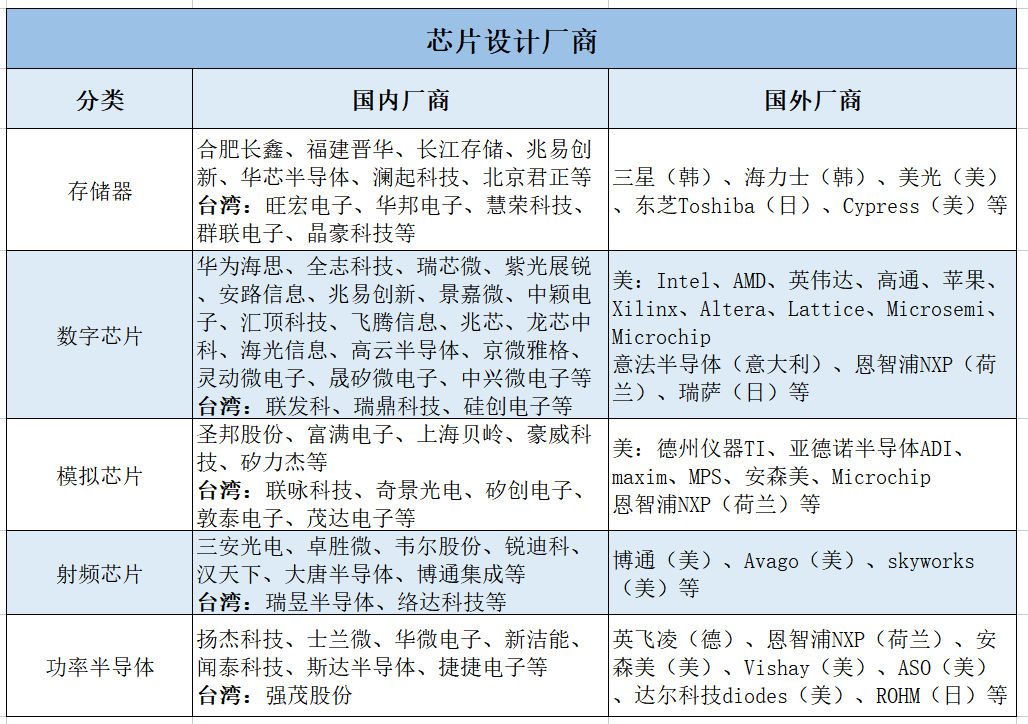
芯片设计行业具有极高的技术壁垒,需要大量的人力、物力投入,且需要较长时间的技术积累和经验积累。我国在芯片设计领域的短板非常明显,高端通用芯片与国外先进水平差距主要体现在中央处理器(CPU)、存储器、高端通用型芯片(包含FPGA、AD/DA等)。目前CPU领域几乎被英特尔垄断了全球市场。存储器领域,主要被三星、海力士、美光等国外厂商垄断。美国在数字芯片设计领域具有明显优势,拥有众多世界顶级的设计公司,如Intel、高通、英伟达、AMD等。此外还有英飞凌、恩智浦、东芝等国际厂商,在芯片设计各细分领域都占有一席之地。
近年来我国芯片设计产业在提升自给率、政策支持、规格升级与创新应用等要素的驱动下,保持了高速成长的趋势。从目前产业的情况看,在射频芯片、存储器芯片、图形处理器(GPU)、通信芯片等领域中,我国有众多优秀的芯片设计厂商崭露头角。例如,在存储器领域,长江存储已经实现了64层3D NAND闪存的量产,并正在研发128层产品;兆易创新在Nor Flash市场份额名列前茅;在射频芯片领域,卓胜微通过不断创新及自主研发,已初步完成射频前端全品类的纵深布局。华为海思和紫光展锐已经是移动通信领域重要的芯片设计厂商,并在产值上进入全球前十大Fabless供应商排名;中兴微电子的RoseFinch7100是中国自主研发的首颗NB-IoT安全物联网芯片;景嘉微是国产GPU市场的主要参与者,也是国内唯一自主研发GPU并用于商用的公司。芯片设计的主要厂商如表6所示。
芯片制造
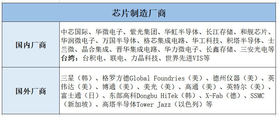
芯片制造是芯片产业链中最核心也最困难的环节,涉及到复杂的工艺流程、精密的设备、高昂的投资和严苛的质量控制。亚洲在芯片制造领域占据领先地位,尤其是中国台湾和韩国,中国台湾的台积电和韩国的三星是全球最大的芯片制造商,拥有领先的制程技术。此外,全球芯片制造商主要代工企业还有联电、格罗方德(Global Foundries)、高塔半导体(Tower jazz)、力晶(Power Chip)、世界先进(VIS)、东部高科(Dongbu HiTek)、X-Fab、SSMC等。目前,中国大陆较为先进的芯片制造商是中芯国际,其最新的14纳米工艺已经开始量产。此外,还有华虹半导体、三安光电、士兰微、华力微电子、长鑫存储、长江存储等一批芯片制造企业,正在悄然发展。尽管我国芯片制造已经达到14纳米及以下制程的水平,但与国际领先水平相比仍存在不小差距。例如,在7纳米及以下工艺上,我国芯片制造企业的产能和品质还难以满足市场需求。同时,受限于高质量的芯片制造设备,我国在芯片制造方面的发展相对滞后,例如,光刻机是芯片制造所需的关键设备,但高端光刻机市场一直被国外垄断。
此外,对于芯片制造环节极其重要的CIM系统(Computer Integrated Manufacture System),也被美国科技巨头IBM和美国半导体设备巨头应用材料所垄断。CIM系统是由生产执行系统(MES)、装备控制平台(EAP)、良率分析控制系统(YMS)、FAB实时调度排产系统(RTS)等数十种软件系统组成,也被称为“制造环节EDA”。市场上产品主要来自IBM和应用材料,其利用先发优势不断增加自身实力,占据12英寸晶圆及以上的主要市场。在此领域国内参与者很少,主要厂商有哥瑞利、上扬软件、赛美特、芯享科技、上海铠铂、格创东智、华经信息等,逐步在6英寸、8英寸、12英寸晶圆厂CIM项目中实现突破。
封装测试
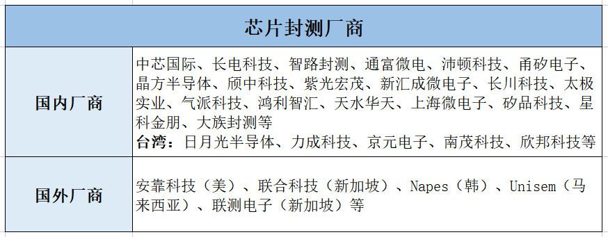
值得一提的是,我国在封装测试领域实力较强,拥有一批具有规模和竞争力的企业。据芯思想研究院数据,2022年全球封测前十强预估排名为:日月光半导体、安靠科技、长电科技、通富微电、力成科技、天水华天科技、智路封测、京元电子、颀邦科技、南茂科技。可以看到,前10名中,仅有第二名安靠科技是美国企业,份额约为14%,另外的9家厂商全部是中国企业,这9家中国企业合计份额达到64%,占了全球近三分之二的封测市场。
国产封装测试企业不仅为国内外客户提供优质服务,也为国内自主创新提供了支撑,并已积累起先进封装技术,其中,球栅阵列封装(BGA)、晶圆级芯片封装(WLCSP)、单列直插式封装(SIP)等先进封装技术已经实现量产。
三、结语
芯片产业投资巨大,竞争激烈,涉及诸多复杂的技术、工艺制程、材料和制造装备。全球芯片产业链是一个持续创新的生态系统,芯片产业链的从业企业需要建立差异化的定位,寻找到自己在产业链中的独特价值和竞争优势。人工智能技术的广泛应用对算力形成巨大的需求,成为芯片产业发展的核心驱动力之一。时间是最客观的见证者,几十年的发展见证了芯片产业的蓬勃发展。在这条没有终点的赛道上,芯片厂商唯有突破技术瓶颈、强化产业链协作,才能劈波斩浪、行稳致远。
翻译:
In recent years, with the rapid development of digital technology and artificial intelligence technology, the application field of chips continues to expand, and its importance in global economic and social development is increasing. The global chip market demand continues to grow, and the industrial chain pattern of the chip industry from design, manufacturing to packaging and testing is rapidly changing, and the industrial chain structure is constantly optimized. This paper will make a brief analysis of the global and Chinese chip industry chain for readers’ reference.
In-depth analysis and interpretation of the chip industry chain
The complete chip industry chain mainly includes the main links of chip design, manufacturing and packaging and testing, and also derives related support industries including chip manufacturing equipment and key materials. According to the upstream and downstream industries, the chip industry chain can be simply divided into: upstream includes EDA software, materials and equipment required for chip manufacturing; The middle reaches are the process of chip design and manufacturing, including chip design, chip manufacturing, package testing; Downstream is widely used in communication equipment, artificial intelligence, automotive electronics, consumer electronics, Internet of Things, industry, medical, military and other fields. As shown in Figure 1:
Among them, EDA software is the core tool of chip design, the support of chip design and manufacturing process, the carrier of chip design methodology, and the link and bridge connecting the two links of design and manufacturing, located in the upstream of the chip industry chain. Associated video
A complete chip design and manufacturing process mainly includes three stages: process platform development, chip design and chip manufacturing. The Process platform development stage is mainly led by fabs. After completing the Design of semiconductor devices and manufacturing processes, the model of semiconductor devices is established and provided to chip design enterprises through PDK (Process Design Kit) or the establishment of IP and standard cell library. The chip design stage is mainly led by the chip design enterprise, which conducts circuit design, simulation verification and physical realization based on the PDK or IP and standard cell library provided by the wafer fab. The chip manufacturing phase is mainly completed by the fab according to the physical realization of the design document.
The above three major stages of design and manufacturing require corresponding EDA tools as support
The above three major stages of design and manufacturing require corresponding EDA tools as support, including manufacturing EDA tools for process platform development and chip manufacturing, and design EDA tools to support the chip design stage.
Chip manufacturing equipment and materials are the other two important support links located in the upstream of the chip industry chain.
In the article “How the chip is” refined “, we simply divide the chip manufacturing process into eight steps: wafer processing, oxidation, lithography, etching, film deposition, interconnection, testing and packaging. The required equipment includes wafer furnace, heat treatment equipment, lithography machine, coating developer, etching equipment, ion implantation equipment, cleaning equipment, film deposition equipment, testing equipment, polishing equipment and so on. In addition, the main materials used in the chip manufacturing process include silicon wafers, electronic special gases, photomask plates, photoresist, polishing materials, high-purity wet electronic chemicals, targets, and packaging materials [1]. The equipment and material types are described in Table 1 and Table 2 below.
Note: In the article “Discussion on chip classification”, we summarize three generations of semiconductor materials according to the classification dimension of semiconductor material types. Silicon and germanium are the first generation materials; Gallium arsenide and indium phosphide are the second generation materials. Silicon carbide and gallium nitride are the third generation materials. Silicon is the most widely used chip material at present, and most common chips are made of silicon. Here we mainly summarize the common materials in chip manufacturing, so only silicon wafers are summarized.
The chip design is located in the middle of the chip industry chain, and the function of the chip can be realized mainly depends on the overall design of the initial chip.
It converts the design of system, logic and performance into a specific physical layout, including the key steps of chip specification formulation, RTL (register transfer level) code implementation, code inspection and analysis, function verification, logic synthesis, layout, static timing analysis, physical verification, power analysis, timing simulation, etc. For more information about the chip design process, see “How are Digital Chips Designed?” One piece.
Packaging and testing is the third specialized link in the middle reaches of the chip industry chain. The main function of the chip package is to provide a durable protective shell for the small, precise and vulnerable chip bare piece, and at the same time, the dense and small electrical signal contacts on the bare piece are connected to the larger electrical signal pins or solder joints outside the package. So that the chip can be easily welded in the electronic components. Chip testing usually consists of two steps: functional testing and performance testing.
Functional testing is the process of checking whether the function of the chip is normal. Usually including checking the input and output of the chip, and whether the logical connection between them is correct. Performance testing is to ensure that the chip has good performance when it is running, including testing the power consumption of the chip, operating speed. Ond other factors that may affect the performance of the chip.
Based on production design and manufacturing capabilities, the chip industry is divided into three operating models: IDM, Fabless and Foundry. The chip industry is an industry with high technical barriers, because chip design and manufacturing include many processes, chip companies are responsible for different links, which has produced different operating models.
Early chip enterprises mainly adopt the IDM model, which is also known as the vertical integration model
Early chip enterprises mainly adopt the IDM model, which is also known as the vertical integration model, that is. The enterprise has both design and manufacturing capabilities [2], and is an industrial operation mode integrating chip design, manufacturing, packaging, testing and sales and other industrial chain links. This industrial model can well cooperate with design, manufacturing and other links to achieve a closed loop of technology, which helps to quickly explore the potential of technology, but its operating costs are high and the return is usually low.
With the development of economy, some IDM enterprises began to give up some production links to independent enterprises to manufacture. And transformed themselves into enterprises that only do design in order to obtain higher profits. This new model, called the vertical division of labor model, separates design, manufacturing and packaging and testing into separate links in the chip industry chain.
Vertical division models include Fabless and Foundry models. Fabless refers to an industrial operation mode that only engages in chip design and sales. But does not involve manufacturing, packaging and testing. This industrial model has low operating costs, small investment scale. And flexible transformation, but it cannot achieve the technical collaborative design of IDM. And it is difficult to complete strict indicators. Foundry is often referred to as a “chip foundry”, which is responsible for the production and manufacture of chips. It is only responsible for one part of the chip manufacturing, packaging or testing, but not responsible for the chip design. This industry model does not bear the risk of decision-making such as market or product design defects. However, the scale of investment is large. And the cost of maintaining the stable operation of the production line is high.
Multi-dimensional interpretation to build the chip industry ecology
The vertical division of labor model derived from the chip industry separates the design and manufacture of chips. However, with the changes in the global economy and the impact of geopolitical factors. The relationship between Fabless manufacturers and Foundry manufacturers is no longer a simple business commission. The fragmentation of the global supply chain forces us to organically combine chip design and manufacturing capabilities to continuously improve the competitiveness of upstream and downstream manufacturers in the independent industrial chain. The chip industry chain can still be tough and develop in an environment full of uncertainty. So, what is the status of the global chip industry chain? What are the typical manufacturers to support each link? The following will focus on the chip industry chain, middle stream analysis.
1. Upstream analysis of the chip industry chain
(1) EDA field
As we all know, the global EDA market is oligopolistic and has a high degree of concentration. Synopsys, Cadence, Siemens EDA (formerly Mentor Graphics, acquired by Siemens in 2016, officially renamed Siemens EDA in 2021) and ANSYS are known as the “four King Kong” of EDA software. Public information shows that its share in the global EDA market is close to 80%.
The monopoly of the “four King Kong” may be due to its ability to provide complete EDA tools, covering the whole set of products from front-end design, back-end design, simulation/verification to the flow sheet, forming a closed loop of design; Or it is because it has worked hard in the areas it is good at, forming unique advantages in different links of the chip design and manufacturing process, and playing a key role. In addition, there are foreign EDA manufacturers. Such as Keysight, Silvaco, Aldec, Altium, Zuken, etc., which continue to deepen their fields of expertise.
Although domestic EDA manufacturers started late, the continuous deepening of the domestic chip industry chain has made the public’s attention to upstream EDA rise sharply.
With the diversified development of the upstream and downstream fields of domestic chips. Especially the accelerated industrialization of emerging technologies such as 5G, artificial intelligence and autonomous driving in recent years. As well as the transformation and upgrading of traditional manufacturing industries. The demand for chips has surged, China’s semiconductor market has flourished. And the domestic EDA demand has grown more rapidly [5]. Under the environment of almost monopoly in foreign countries, a number of independent EDA manufacturers were born in China, represented by Huada Jiutian, Gaolun Electronics, Guangliwei, Guowei Sier Core, Core Vision, core Huazhang, Ruobei Electronics, full core Intelligence manufacturing, Jiutongfang microelectronics, core and semiconductor. As a result, many excellent EDA unit software have emerged, and the manufacturers are developing towards local solutions and whole process solutions by virtue of their advantages in the subdivision field.
(2) Chip manufacturing equipment
Chip devices usually have three characteristics. First, the research and development time is long, the research and development of a new equipment is less than five years, more than ten years. But also need to continuously improve and optimize in the process of use. Second, the amount of investment is large, for example, the Dutch lithography giant ASML has spent more than 2 billion euros per year for 20 consecutive years to develop EUV equipment. Three is a high degree of monopoly, the United States, Japan and Europe five giants leading the global semiconductor equipment market, respectively, Applied Materials (Applied Materials), ASML (ASML), Lam Research (LAM), Tokyo Electron (Tokyo Electron), KLA semiconductor (KLA).
For example, the Dutch ASML has more than 90% market share in the lithography market. Especially in the field of extreme ultraviolet lithography (EUV) in an absolute monopoly position. American applied materials in the field of ion etching and film deposition are industry leaders. In the field of etching, cleaning, ion implantation equipment. It also occupies a place; Panglin Semiconductor is the world’s leading enterprise in etching equipment.
In recent years, the national policy focus on support, domestic chip equipment manufacturers have gradually developed.
In the various subdivisions of chip equipment, polishing equipment, cleaning equipment, etching equipment, physical vapor deposition (PVD) equipment, etc., have achieved breakthroughs from 0 to 1. Smic 12 inch etching machine has been successfully used in TSMC 5nm production; Shengmei Semiconductor cleaning equipment has entered a number of domestic production lines; The ion implantation equipment of China Electronics has successfully realized the localization of the whole spectrum of ion implantation machine products; Huahai Qing’s chemical-mechanical polishing (CMP) equipment has achieved full coverage of all 28nm process processes; Xinyuan Micro’s lithographic process coating equipment and single chip wet process equipment have been used as mainstream models in TSMC, Changdian Technology, Huatian Technology, Tongfu Micro Power and other domestic first-line manufacturers. The major manufacturers in each segment of chip equipment are shown in Table 4.
(3) Chip manufacturing material
According to the chip production process, materials and equipment are the physical basis of chip manufacturing. And the output scale of raw materials is directly related to the development of the chip industry. From the current situation of domestic industrial development, China’s chip material is a relatively weak link in the industrial chain. Mainly because the industry started late, and it is at a disadvantage in terms of category richness and competitiveness.
For example, the global silicon wafer market is mainly dominated by a few manufacturers such as Shin-Etsu and SUMCO. And China’s silicon wafer industry started late, at present, domestic silicon wafer suppliers are mainly concentrated in the supply of 8-inch and below silicon wafers, which can not meet the mainstream demand; The photomask market is mainly dominated by leading enterprises in the United States and Japan, and the industry concentration is high, and the top three photomask manufacturers in the world are Photronics in the United States, Dai Nippon Printing in Japan and Toppan in Japan.
With the continuous large-scale construction of the domestic chip market, domestic chip materials have ushered in rapid development.
At the same time, relying on industrial policy guidance and product price advantages, local enterprises have made breakthroughs in their respective fields. For example, Shanghai Silicon industry has mastered the complete set of core technologies for the production of silicon wafers. Including 300mm silicon wafers; Germanane, high-purity ethylene, high-purity propylene and other products of Walter Gas have made application breakthroughs in the field of electronic special gas, especially high-end chip materials; Our target products have been applied to the most advanced manufacturing processes of the world famous semiconductor manufacturers represented by TSMC. Anji Technology has successfully broken the monopoly of foreign manufacturers on chemical mechanical polishing liquid. Some functional wet electronic chemicals, electroplating solution and additives in the field of integrated circuits. And the three core products have achieved technological breakthroughs in specific fields. The major manufacturers in each segment of chip materials are shown in Table 5.
2. Middle stream analysis of chip industry chain
(1) Chip design
The chip design industry has extremely high technical barriers, requires a lot of manpower and material input. And requires a long period of technology accumulation and experience accumulation. China’s shortcomings in the field of chip design are very obvious. And the gap between high-end general purpose chips and foreign advanced levels is mainly reflected in central processing unit (CPU), memory, high-end general purpose chips (including FPGA, AD/DA, etc.).
At present, the CPU field is almost monopolized by Intel in the global market. In the field of memory, it is mainly monopolized by foreign manufacturers such as Samsung, Hynix and Micron. The United States has obvious advantages in the field of digital chip design. With many of the world’s top design companies, such as Intel, Qualcomm, Nvidia, AMD and so on. In addition, there are international manufacturers such as Infineon, NXP, and Toshiba. Which have a presence in various segments of chip design.
In recent years, China’s chip design industry has maintained a rapid growth trend driven by factors such as improving self-sufficiency, policy support, specification upgrading and innovative applications.
From the current industry situation, in the field of RF chips, memory chips, graphics processors (Gpus), communication chips, etc. There are many excellent chip design manufacturers in China. For example, in the memory field, Changjiang Storage has realized the mass production of 64 layers of 3D NAND flash memory. And is developing 128 layers of products; Zhaoyi Innovation ranks first in Nor Flash market share. In the field of RF chips, Zhuosheng Micro has initially completed the in-depth layout of the whole category of RF front-end through continuous innovation and independent research and development.
Huawei hisilicon and Unigroup Zhanrui are already important chip design manufacturers in the field of mobile communications. And have entered the world’s top ten Fabless suppliers in terms of output value. Zte Microelectronics’ RoseFinch7100 is the first NB-IoT secure Internet of Things chip independently developed in China. Jingjiawei is a major player in the domestic GPU market and the only company in China that independently develops and uses Gpus for commercial use. The main manufacturers of chip design are shown in Table 6.
(2) Chip manufacturing
Chip manufacturing is the core and most difficult link in the chip industry chain, involving complex process flow, precision equipment, high investment and strict quality control. Asia leads the way in chip manufacturing, especially Taiwan and South Korea, where Taiwan’s TSMC and South Korea’s Samsung are the world’s largest chipmakers with leading process technology. In addition, the major foundry companies of Global Chip manufacturers are UMC, Global Foundries, Tower jazz, Power Chip, World Advanced (VIS), Dongbu HiTek, X-Fab, SSMC and so on. At present, the more advanced chip manufacturer in mainland China is SMIC, And its latest 14-nanometer process has begun mass production.
In addition, there are a number of chip manufacturing enterprises such as Huahong Semiconductor, SAN ‘an Optoelectronics, Shilanwei, Hualimicro Electronics, Changxin Storage, Yangtze River Storage, etc., which are quietly developing. Although China’s chip manufacturing has reached the level of 14 nm and below the process. There is still a big gap compared with the international leading level. For example, in the process of 7 nm and below. The capacity and quality of China’s chip manufacturing enterprises are still difficult to meet market demand. At the same time, limited by high-quality chip manufacturing equipment, China’s development in chip manufacturing is relatively lagging behind. For example, lithography machine is the key equipment required for chip manufacturing. But the high-end lithography machine market has been monopolized by foreign countries.
In addition
In addition, the CIM System (Computer Integrated Manufacture System), which is extremely important for the chip manufacturing process. It is also monopolized by the US technology giant IBM and the US semiconductor equipment giant Applied Materials. CIM system is composed of production execution system (MES), equipment control platform (EAP), yield analysis control system (YMS), FAB real-time scheduling system (RTS) and other dozens of software systems, also known as “manufacturing EDA”. The products in the market are mainly from IBM and Applied Materials. Which use the first-mover advantage to continue to increase its own strength, occupying the main market of 12-inch wafers and above. In this field, there are few domestic players. The main manufacturers are Gorelli, Upsoftware, Semet, Xinxiang Technology, Shanghai Jibao, Gechuang East Intelligence, Huajing Information, etc. And gradually achieve breakthroughs in the 6-inch, 8-inch, 12-inch fabs CIM project.
(3) Package test
It is worth mentioning that China has a strong strength in the field of packaging and testing. And has a number of enterprises with scale and competitiveness. According to core thought research Institute data, the world’s top ten sealed test estimates in 2022 are:. ASE Semiconductor, An technology, Changdian Technology, Tongfu micro electricity, Licheng Technology, Tianshui Huatian Technology, Zhilu sealed test, Jingyuan Electronics, Chi Bang Technology, Nanmao Technology. It can be seen that among the top 10, only the second Anrely Technology is an American enterprise. With a share of about 14%, and the other nine manufacturers are all Chinese enterprises. With a total share of 64% of these nine Chinese enterprises, accounting for nearly two-thirds of the global closed test market.
Domestic packaging and testing enterprises not only provide quality services for domestic and foreign customers. But also provide support for domestic independent innovation, and have accumulated advanced packaging technology. Among which, ball grid array package (BGA), wafer-level chip package (WLCSP), single-line in-line package (SIP) and other advanced packaging technology has been mass produced.
Conclusion
The chip industry has huge investment and fierce competition, involving many complex technologies, processes, materials and manufacturing equipment. The global chip industry chain is an ecosystem of continuous innovation. And enterprises in the chip industry chain need to establish a differentiated positioning and find their unique value and competitive advantage in the industry chain. The wide application of artificial intelligence technology has formed a huge demand for computing power and has become one of the core driving forces for the development of the chip industry. Time is the most objective witness, and decades of development have witnessed the vigorous development of the chip industry. On this track with no end, chip manufacturers can only break through the technical bottleneck and strengthen the industrial chain collaboration in order to split the waves and move steadily.
本文由数字化转型网(www.szhzxw.cn)转载而成,来源于数字化企业;编辑/翻译:数字化转型网宁檬树。

免责声明: 本网站(https://www.szhzxw.cn/)内容主要来自原创、合作媒体供稿和第三方投稿,凡在本网站出现的信息,均仅供参考。本网站将尽力确保所提供信息的准确性及可靠性,但不保证有关资料的准确性及可靠性,读者在使用前请进一步核实,并对任何自主决定的行为负责。本网站对有关资料所引致的错误、不确或遗漏,概不负任何法律责任。
本网站刊载的所有内容(包括但不仅限文字、图片、LOGO、音频、视频、软件、程序等) 版权归原作者所有。任何单位或个人认为本网站中的内容可能涉嫌侵犯其知识产权或存在不实内容时,请及时通知本站,予以删除。